- 您现在的位置:买卖IC网 > Sheet目录323 > DV164039 (Microchip Technology)KIT DEV PIC24FJ256DA210
�� �
�
�PIC24FJ256DA210� Development� Board� User’s� Guide�
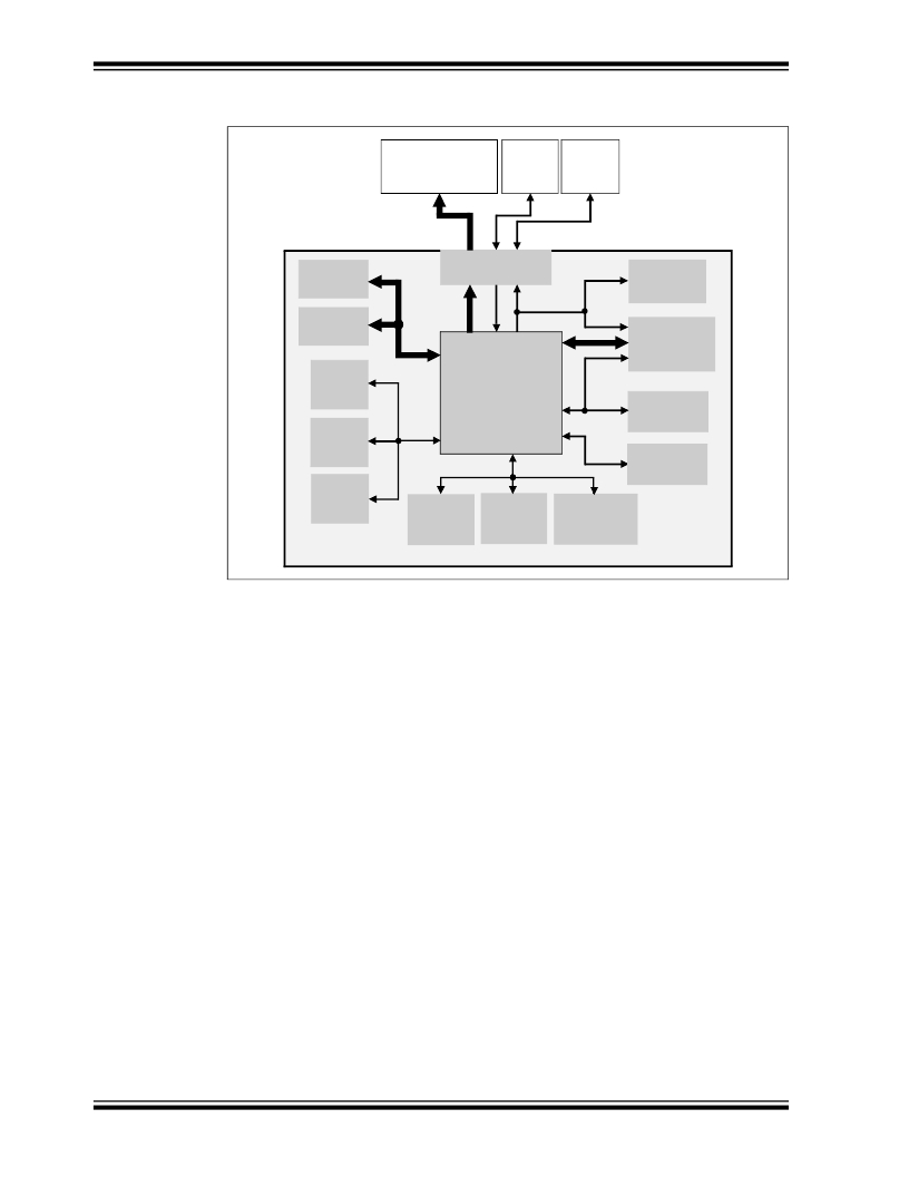
�FIGURE� 4-1:�
�PIC24FJ256DA210� DEVELOPMENT� BOARD� BLOCK�
�DIAGRAM�
�Display� Panel�
�(TFT,� CSTN,� MSTN)�
�Resistive�
�Touch�
�Screen�
�Display�
�SPI�
�DISPLAY�
�512� KByte�
�SRAM�
�Connector�
�SPI� FLASH�
�(16MBit)�
�SPI�
�512� Kbyte�
�FLASH�
�USB�
�EPMP�
�PICtail?� Plus�
�Connector�
�Host�
�PIC24FJ256DA210�
�UART�
�RS-232�
�Transceiver�
�USB�
�USB�
�Device�
�ICSP?�
�OTG�
�USB�
�3� CTMU/�
�4� LEDs�
�3� Buttons/�
�Switches�
�R3�
�Potentiometer�
�4.3�
�GENERAL� HARDWARE� FEATURES�
�4.3.1�
�PCB� Layout�
�The� PIC24FJ256DA210� Development� Board� uses� several� design� strategies� to� provide�
�a� stable� demonstration� and� development� environment.� Users� should� note� these�
�features� and� design� tips� when� developing� their� own� graphic� applications.�
�The� development� board� uses� a� four-layer� PCB� design;� this� allows� high-frequency�
�signals� to� be� routed� in� a� way� to� avoid� crosstalk� between� data� signals.� It� also� gives�
�additional� noise� protection� due� to� improved� grounding.�
�For� additional� noise� protection,� oscillator� circuits� and� crystals� are� laid� out� with� appro-�
�priate� grounding� and� guard� rings.� The� layout� guidelines� are� described� in� Section� 2.�
�“Guidelines� for� Getting� Started� with� 16-Bit� Microcontrollers”� of� the� device� data�
�sheet.�
�Each� group� of� color� signals� (Red,� Green� and� Blue)� is� routed� together� to� reduce� inter-�
�color� crosstalk.� This� means,� for� example,� that� Red� signals� are� close� together� and� do�
�not� mix� with� Green� and/or� Blue� signals.� Ideally,� it� is� recommended� to� run� a� ground� wire�
�or� trace� between� groups� of� color� signals� to� reduce� crosstalk.� Also,� the� traces� for� color�
�data� should� be� as� close� to� equal� length� as� possible,� and� avoid� the� use� of� vias� wherever�
�possible.�
�4.3.2�
�Microcontroller�
�The� development� board� is� supplied� with� the� PIC24FJ256DA210� microcontroller�
�directly� soldered� to� the� board� at� U2.� The� device� is� installed� with� the� notched� corner� (pin�
�1)� oriented� to� the� lower� right.� Vias� are� provided� around� the� device,� which� allow� access�
�to� all� microcontroller� signals;� this� is� labelled� on� the� board� as� U9.� A� riser� may� be� installed�
�here� to� facilitate� connections� to� user� added� components� in� the� prototyping� area.�
�DS51911A-page� 32�
�?� 2010� Microchip� Technology� Inc.�
�发布紧急采购,3分钟左右您将得到回复。
相关PDF资料
DV164101
KIT DEV PICKIT1 FLASH 8/14PIN
DV164120
KIT STARTER PICKIT 2
DV164121
KIT PICKIT 2 DEBUG EXPRESS
DV164122
ANALYZER SRL PICKIT W/DEMO BOARD
DV164131
KIT STARTER PICKIT 3
DV164132
KIT EVAL F1 FOR PIC12F1/PIC16F1
DV243003
KIT STARTER FOR SRL MEM PRODUCTS
DVA1001
ADAPTER FOR PIC16F716 18DIP
相关代理商/技术参数
DV164101
功能描述:开发板和工具包 - PIC / DSPIC PICkit 1 8/14P Flash RoHS:否 制造商:Microchip Technology 产品:Starter Kits 工具用于评估:chipKIT 核心:Uno32 接口类型: 工作电源电压:
DV164101
制造商:Microchip Technology Inc 功能描述:TOOLS: FLASH MICROCONTROLLER (
DV164102
功能描述:开发板和工具包 - 无线 rfPICkit RoHS:否 制造商:Arduino 产品:Evaluation Boards 工具用于评估:AT32UC3L 核心:AVR32 频率: 接口类型:USB 工作电源电压:5 V
DV164120
功能描述:电路内置调试器 PICkit 2 8/14/20P Flash RoHS:否 制造商:Microchip Technology 产品:In-Circuit Debugger Kits 工具用于评估:PIC MCUs, dsPIC DSCs 用于:07-00024, AC164113 核心:dsPIC, PIC 接口类型:USB 工作电源电压:3 V to 5 V
DV164121
功能描述:电路内置调试器 PICkit 2 Debug Express RoHS:否 制造商:Microchip Technology 产品:In-Circuit Debugger Kits 工具用于评估:PIC MCUs, dsPIC DSCs 用于:07-00024, AC164113 核心:dsPIC, PIC 接口类型:USB 工作电源电压:3 V to 5 V
DV164121
制造商:Microchip Technology Inc 功能描述:ICPICKIT2 PROGRAMMER/DEBUGGER ((NW))
DV164121+TEFLCST3
制造商:Microchip Technology Inc 功能描述:KIT PICKIT2+FLOWCODE-HOME BUNDLE 制造商:Microchip Technology Inc 功能描述:ICD, PICKIT 2, FLOW CODE, PIC, DSPIC 制造商:Microchip Technology Inc 功能描述:ICD, PICKIT 2, DEBUG EXP, FLOW CODE, PIC, DSPIC; Silicon Family Name:PIC12F6xx, PIC16F5xx; Core Architecture:PIC; Core Sub-Architecture:PIC12, PIC18, PIC24; IC Product Type:Debugger / Programmer; Series:PICkit 2 ;RoHS Compliant: Yes
DV164122
功能描述:界面开发工具 PICkit Ser Analyzer RoHS:否 制造商:Bourns 产品:Evaluation Boards 类型:RS-485 工具用于评估:ADM3485E 接口类型:RS-485 工作电源电压:3.3 V